An Overview of the Semiconductor Industry
A primer on the various market segments & market leaders across the industry
Table of contents
The Basics
Electronic Design Automation
Instruction Set Architectures
Manufacturing
The Process
Foundries
Manufacturing Equipment
Chip Markets
Logic
Memory
Analog
Conclusion
Disclaimers:
This is not investment advice; you should do your own research before investing.
Introduction
My motivation to write this article came from two key principles of my investing philosophy:
The best companies are those who act as a monopoly or semi-monopoly in a growing industry with great leadership.
I want to deeply understand the technology of the companies I invest in so I can understand the potential for innovation or disruption.
Consistently, I see semiconductor companies fit the criteria of point one. However, I didn’t invest because of my lack of understanding of the technology.
I have a few goals of this article:
To provide readers with a fundamental understanding of the semiconductor industry.
To identify opportunities for investment in companies that I can reasonably predict the future of.
To create graphics that make the most complex industry in the world a little less intimidating (ergo the friendly font).
Let’s commence:
The Basics
Design vs Manufacturing
Essentially, the semiconductor industry can be broken into two segments: Design & Manufacturing.
A company that designs semiconductors but doesn’t manufacture them is considered a fabless firm.
A company that only does manufacturing, based on the designs provided by fabless firms, is called a foundry.
A company that does both the design and manufacturing of semiconductors is an Integrated Device Manufacturer or IDM.
The Design Process
Semiconductor Design is exceptionally complex. Apple’s most advanced chip has 134 billion transistors (building blocks of chips, a “gate” that can pass on an electric charge).
The design process identifies the requirements of the chip, lays out the logic design of the chip, simulates the performance, and tests for errors. That process is repeated until the chip is flawless.
The software used for this process is called Electronic Design Automation (EDA) software.
Once a design is complete, it’s then sent to foundries for manufacturing.
The Architecture
There are three basic architectures used to design processors: Arm (recently IPO-ed), x86 (developed by Intel), and RISC-V (an open-source alternative).
A CPU is the main processor built on these architectures.
These architectures provide a bridge between the hardware of the chip and the software used to program the chips.
x86 is proprietary IP developed by Intel. AMD reverse-engineered Intel’s products to develop their own x86 chips.
Arm’s architecture is proprietary IP they license out to other firms.
RISC-V is developed by the RISC-V international organization and open for anyone to use.
The Manufacturing Process
Semiconductor manufacturing is the most complex process on the planet.
Foundries are at the center of the manufacturing process, most of which are in Taiwan.
Those foundries use a variety of tools in the process, mostly made by 5 companies: Applied Materials, ASML, Tokyo Electron, KLA Corporation, and Lam Research.
The basic flow is this:
It’s okay if this process doesn’t make total sense; few people in the world fully understand the process end-to-end.
Types of Chips
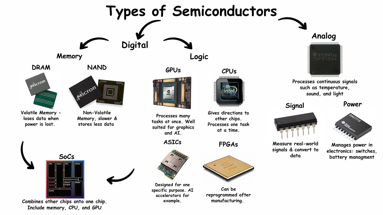
There are two types of chips: digital chips and analog chips. Digital chips are based on binary values, 1 or 0. Analog chips take continuous signals such as sound or light.
Digital chips are more complex and make up most of the chips you’re familiar with. Analog chips process basic functions like telling a flashlight to turn on when you hit press the button.
The digital chip market can be divided into two categories: logic chips and memory chips.
A few other types of chips exist application-specific integrated circuits (ASICs), Field Programmable Gate Arrays, and system-on-a-chip devices (SoCs).
Logic Chips:
Logic chips process information to complete a task. CPUs and GPUs are the two most common examples.
Central Processing Units (CPU): CPUs are the main chips in a computer responsible for carrying out tasks. They’re often called the “brains” of the computer. CPUs handle the majority of the instructions from both the software and hardware of a computer. It’s important to note that a single CPU processor can only handle one task at a time.
Graphics Processing Units (GPUs): GPUs are chips designed for parallel processing or running many tasks at once. This works well for graphics processing where a computer has to process many pieces of data at once. It also works well for AI because AI requires massive amounts of low-complexity calculations at the same time. While GPUs can’t handle the complexity of problems that a CPU can, software can breakdown those problems into pieces GPUs can handle.
Most of the companies you’re familiar with create logic chips as these act as the ‘brains’ of technology.
Memory Chips:
Memory chips are designed to store data. There are two types of them:
DRAM: DRAM chips are ‘volatile’ memory chips which means their data is lost when the power source to the chip is turned off. DRAM offers larger store capacity and faster speeds. DRAM is used when fast processing speed is required.
NAND: NAND chips are non-volatile memory chips that preserve saved data when the power is turned off. NAND chips are used when data must be permanently saved.
Others:
Application-specific integrated circuits (ASICs): ASICs are chips designed for one specific purpose. For example, Google’s chips (TPUs) are designed specifically as AI accelerators.
Field Programmable Gate Arrays: FPGAs are chips that can be re-programmed after manufacturing.
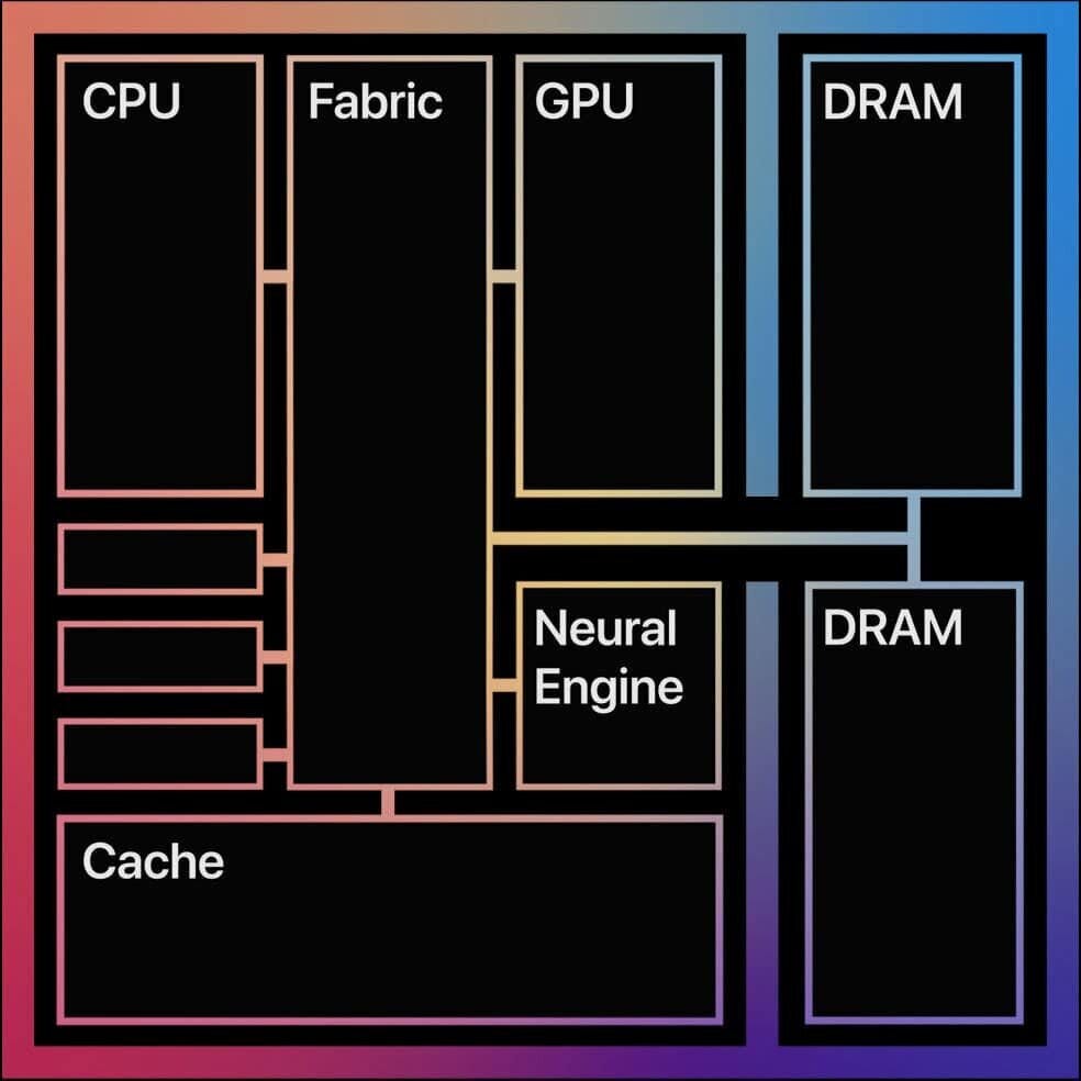
System-on-a-chip devices (SoCs): SoCs put multiple types of chips into one chips multiple types of chips into one. For example, here’s a diagram of Apple’s mac M2 SoC:
Electronic Design Automation
EDA tools provide the software which companies use to design chips before sending them to the foundries.
Before chips are manufactured, they must go through a number of design steps and check for errors after each step. A single design flaw will result in millions of lost dollars. This error-checking process is called verification.
Virtually any company designing their own chips will use Synopsys or Cadence Design Systems or both.
The EDA market is also tightly coupled with the Semi Design Intellectual Property market, where companies sell pre-designed chips.
The IP acts as “drag-and-drop” blocks to integrate into a customer’s chip design.
Market Overview
The market is oligopolistic with Synopsys, Cadence Design Systems, and Siemens EDA (formerly mentor graphics).
As chip design complexity increases, the market is becoming even more concentrated.
The market has grown at a 9.6% CAGR over the last 12 years with that growth accelerating over the last 5 years at a 12.2% CAGR.
There are two driving forces for the growth of the EDA market:
Increasing chip complexity:
As chips become more complex, the design tools become even more important. Chip manufacturing costs are increasing which makes flaws even more expensive. The design and validation of these chips must be perfect. Increasingly, AI is playing a role in optimizing these chips and preventing flaws.
With greater complexity comes more advanced tooling which is more expensive.
With that being said, even the EDA market leaders are struggling to keep up with semiconductor complexity.
This has been a known problem since the 1990s, but here’s the gist of it:
Semiconductor complexity is growing faster than the design tools can keep up with. The design tools’ complexity are growing faster than the verification tools can keep up with.
This is why we’re seeing continued consolidation of the EDA market. Complexity is pushing out smaller EDA players.
Asianometry has a good video if you’re interested in learning more about this problem.
Increasing number of fabless firms
Here’s a list of some non-chip companies designing their own semiconductors:
Apple
Amazon
Google
Microsoft
Tesla
IBM
Meta
Ford
GM
As it becomes harder to get efficiency gains out of new generations of chips, companies are designing their own to optimize chips for their own processes. It also gives them greater control over their own supply chain. The competitive advantages are clear with Apple’s M2 chips performing well against competition. Amazon is toting their cost efficiency with their data center chips.
Every new company designing their own chips goes through Synopsys and/or Cadence.
EDA essentially encompasses the entire design phase and partners closely with foundries to make the manufacturing process as efficient as possible.
Instruction Set Architecture
The ISA essentially acts as an interface between the hardware and the software.
It defines the set of commands that the hardware can perform such as instructions, data types, and memory settings.
There are really only 3 options for architectures in the industry: Arm, x86, and RISC-V.
First, the business model is different for all three. Arm licenses their IP, x86 is only developed by Intel & AMD, and RISC-V licenses are free. Companies can then license out their own RISC-V IP once they develop
Arm
Arm, the company, was originally founded as a joint venture with Apple. They own the IP with their ISA and license that out to other companies.
Arm also refers to the architecture that the company Arms licenses out. The r in arm stands for RISC, or reduced instruction set computer. It means that they require a much smaller instruction set whereas x86 can be given a much more extensive instruction set. Arm is much more energy efficient & produces less heat. This is why the entire smartphone industry runs on Arm. However, Arm processors are becoming more powerful and x86 processors are becoming more efficient.
Arm has steadily been taking market share from x86. Most of this can be attributed to Apple’s Arm processors taking share.
x86
x86 was developed by Intel and was the dominant ISA for the majority of the industry’s history. It is still used in most desktop and laptop computers today.
As mentioned above, x86 can be given a much more extensive instruction set. In turn, x86 can handle more complex workloads. Traditionally, this has meant that the x86 chips were more powerful; however, the most powerful supercomputer in the world is now based on Arm.
RISC-V:
Arm & RISC-V fundamentally offer similar architectures, as both are RISC designs.
So why choose one or the other?
It comes down to the open-source vs closed-source debate that’s been waging on since the beginning of the technology era.
Arm optimizes their architecture to make life easy for their customers. They invest in R&D to continue to improve their product and offer new innovations. It also provides an industry standard for adjacent companies to build around.
RISC-V provides full customization. Companies can specialize their chips around an ISA designed for their processes. Customers don’t have to pay royalties and licensing fees for their products. It also takes additional expertise to develop custom architectures, and semiconductor expertise is hard to come by.
Manufacturing
Semiconductor manufacturing is likely the most complex process on the planet.
If you’re going to invest in semiconductors, it’s important to understand the general process of how semiconductors are manufactured.
Here’s a video from Asianometry that does a good job if you want a more detailed approach.
The Process
The basic flow is this:
Tracking/Cleaning
Tracking: ensuring that each wafer moves through the process in the correct order.
Cleaning: removing any contaminants from the surface of the water before processing.
Deposition (Step 1 above)
Deposition coats the wafer with the necessary materials to create transistors.
Chemical Vapor Deposition (CVD): Process used to create films on a substrate. Deposits thin layer of material onto the water’s surface.
Physical Vapor Deposition (PVD): Another method used for depositing films.
Epitaxy/Other deposition: A process used to grow a crystalline layer on a crystalline substrate. Used to create layers with specific electrical properties.
Photoresist Coating (Step 1)
Wafer is then covered with a light-sensitive coating that can be dissolved through the lithography process.
Lithography (Step 2)
Wafer is inserted into a lithography machine where light is magnified onto the chip in the pattern of the semiconductor. This solidifies the portions of the photoresist that are going to stay.
Etching (Steps 3 and 4)
Wafer is baked and developed to remove the exposed photoresist.
Etching removes the rest of the non-patterned portions of the photoresist through chemicals and gases.
Ion Implantation (Step 5)
Wafers are bombarded with ions, positive or negative, to create the electrical properties of a semiconductor.
Then steps 2 through 5 are repeated until there’s a sufficient amount of layers.
Metal Interconnects (Step 6)
Using another deposition process, metal wiring is added to allow electrical signals to be processed through the circuits.
Packaging
The wafers are then sliced into ‘dies’, are bonded onto a base called a substrate, then a ‘lid’ is added creating the semiconductors we recognize.
Foundries
TSMC dominates the foundry market.
Samsung has a respectable footprint as well. Together, TSMC and Samsung account for ~71% of the foundry market.
TSMC and Samsung are the only two companies making the most advanced semiconductors in the world.
SMIC is China’s biggest semiconductor foundry, the Chinese government is investing heavily in their capabilities to reduce reliance on Taiwan and the West.
UMC is another Taiwanese chip company, but they only manufacture 22/28nm technology (more on this below)
GlobalFoundries, formerly AMD’s foundry, makes up to 12nm technology.
Intel is the wild card in the foundry market. They are currently building out Intel Foundry Services.
They are the only other company in the world that can compete with TSMC and Samsung on the most advanced processes.
They have reportedly signed a few large customers for their most advanced node, but that won’t be in production until 2025.
Node Technology
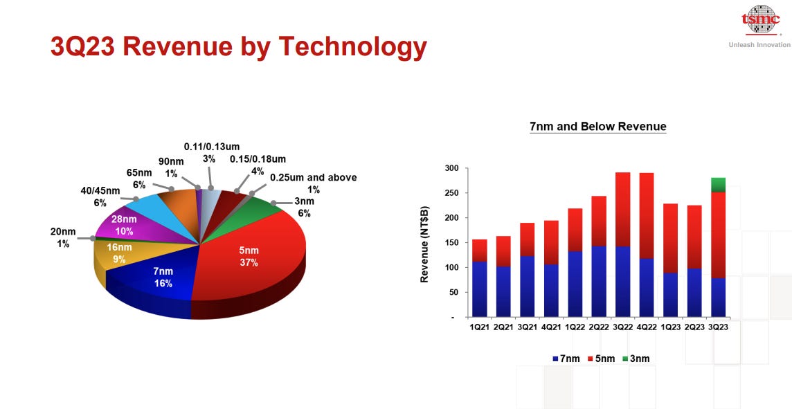
You’ll see the complexity of a chip defined in nanometers or ‘nm’. This used to refer to actual measurements on the chip, but now it’s just a marketing term. However, it does give us a general idea of the complexity of semiconductors each company is making.
For example, here’s the revenue breakdown for TSMC’s latest quarter:
Why is this important? Only two companies, Samsung and TSMC, have 5nm process chips available to the market. TSMC started selling 3nm chips last quarter. Samsung has produced 3nm chips, but they are only used in certain technologies. There are rumors about significant challenges for Samsung’s manufacturing process.
Intel and SMIC reportedly have 5nm chips in production for their foundries.
No other companies in the world are even trying to make this technology, it’s too expensive and too complicated.
International Expansion
In an effort to diversify their business and de-escalate the focus on Taiwan, TSMC is building fabs across the world.
USA: TSMC is building a $40B, 5-nm/3-nm plant in Arizona which will supply over 600,000 wafers annually to large US customers including Apple & Nvidia.
Germany: TSMC is building an $11B, 28-nm/22-nm fab in Dresden to supply 480,000 wafers to German auto & industrial companies.
Japan: TSMC is building two fabs in Japan. The first is a $7B 28-nm/22-nm fab in Kumamoto with annual capacity of 540,000 wafers. The second fab will be $7.4B and focused on manufacturing 5-nm/10-nm chips expected to be complete in the latter half of this decade.
China: TSMC has one fab in China that they are working to upgrade. The US and its allies are preventing them from building new fabs in China.
Outside of TSMC, a number of firms are building fabs in the United States.
Manufacturing Equipment
Like the other steps of the manufacturing process, each tool industry is dominated by just a few companies.
These are some of the largest companies in the world, all with market caps over $50B and revenue over $10B.
ASML: Lithography
ASML is one of the few true monopolies on the planet, primarily due to the wild complexity of lithography machines.
Lithography is the process of etching transistors on silicon wafers.
To give you an idea of how complex it is, here’s a summary of the technology: A high-energy laser fires on a microscopic piece of tin, turning it into plasma, emitting a ray of ultraviolet light, which is then magnified into one beam of ultraviolet light, then reflected across a number of mirrors, then reflected off a photomask with the design of the semiconductor circuits, it’s then reflected onto atomically sized chips on the wafer, which burns the pattern onto the photoresist of the wafer. After it’s developed, the wafer is cleaned. This process is repeated many times until a fully functioning chip design is etched onto the wafer.
Few people in the world fully understand this technology. The top-end lithography machines have over 100,000 parts. It takes four 747s to ship one to a customer. ASML only makes ~55 of them a year. There’s a reason why these machines cost $200m-$300m a piece.
The others: Applied Materials, Tokyo Electron, Lam Research, KLA Corporation
This is a great image highlighting the steps of the manufacturing process and who they’re dominated by:
Feel free to refer back to the segment intro for descriptions of the categories (lithography, tracking/cleaning, chemical vapor deposition, physical vapor deposition, epitaxy/other deposition, etching, chemical mechanical polishing, thermal, ion implantation, process diagnostics & control, electrochemical deposition.
Applied Materials makes machines across the manufacturing process including deposition, implantation, and epitaxy tools.
Lam Research Corporation is the largest etching equipment provider. They also offer deposition tooling.
KLA Corporation dominates the process diagnostics and control space.
Tokyo Electron is exposed to most of the same markets as Applied Materials. The two companies tried to merge in 2015, but plans were prevented by regulators.
All of these companies have high market share in their respective markets, high-margins, and strong moats.
Device Manufacturing
After the chips are made, the next step is manufacturing whatever device the chips are going to be made into.
For example, Apple has TSMC manufacture the chips in their iPhone. Then, those chips (along with the other components of an iPhone) are sent to Foxconn to assemble the iPhone.
Foxconn, also based out of Taiwan, is the largest device manufacturer in the world. They reportedly make over 70% of Nvidia’s GPUs and all of Apple’s iPhones.
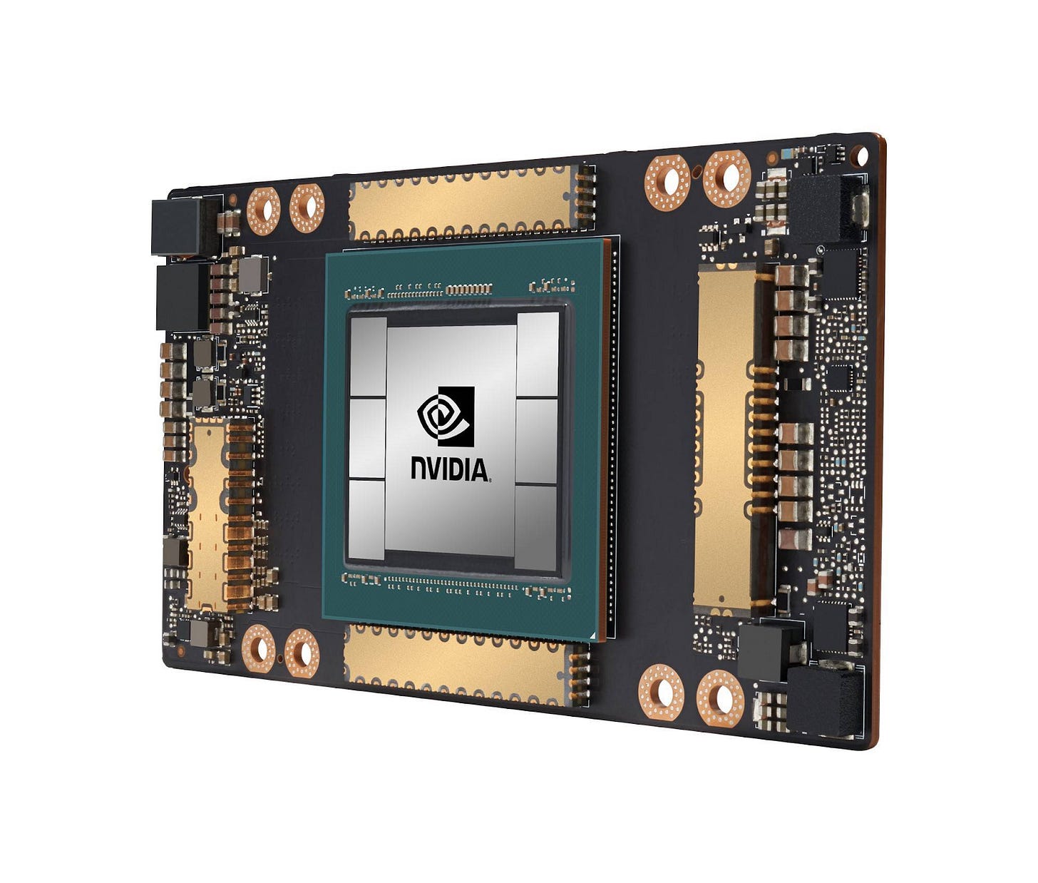
To visualize this, here’s a Nvidia data center GPU:
TSMC makes the large chip in the middle. However, Foxconn attaches it to the baseboard and assembles the other components.
Chip Markets
The intent of this section is to provide a high-level understanding of the market share & major players across the different segments of the industry.
GPU
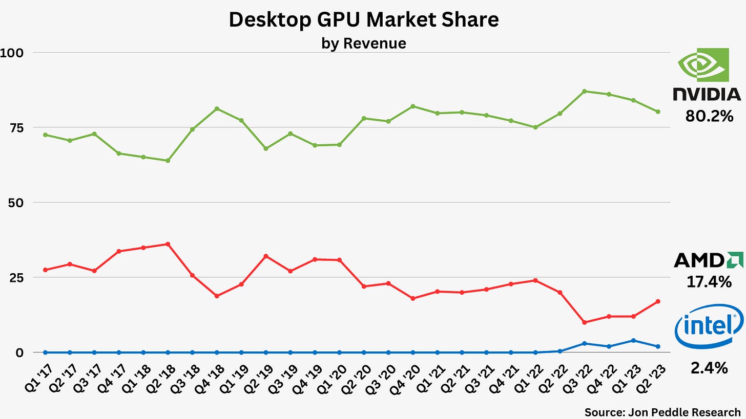
Nvidia dominates the GPU market, with AMD in second place, and Intel in a distant 3rd place.
There are three primary revenue streams for the GPU market. The PC market where GPUs process the graphics for computers. The data center market where GPUs are becoming increasingly important for AI processing. Finally, the gaming market where GPUs used to specialize in.
PC market share
Data Center Market Share
There are really only two makers of GPUs for data centers as well, Nvidia and AMD. Nvidia’s GPUs have exploded this year while AMD’s datacenter GPU is launching next quarter.
Overall market share for data center across Nvidia, Intel, and AMD is below:
Nvidia Overview
The hottest company in the world (for a good reason). Nvidia’s business is built on GPUs, they then customize those GPUs for specific applications.
Nvidia designs semiconductors serving 4 markets:
Data Center: This is where the massive growth of Nvidia’s business has come from. Nvidia GPUs are the best suited chips in the world for AI workloads.
Gaming: Nvidia’s original business. Graphics were well suited for their technology because it requires a chip to process many processes at once.
Automotive: Nvidia GPUs are the industry leader in autonomous vehicle processing. Tesla is a huge customer.
Professional Visualization: Includes enabling the creation of digital twins for companies & enabling the metaverse.
AMD Overview
AMD has a broader offering than Nvidia. They design both CPUS & GPUS, as well as FPGAs & SoCs. They focus on four markets:
Data Center: They make both CPUs and GPUs for data centers, competing with Intel & Nvidia.
Client: CPUs for personal computers competing with Intel.
Gaming: GPUs for gaming competing with Nvidia.
Embedded: CPUs and GPUs for products in industry (automobiles, medical devices, aerospace products etc.)
They aren’t the market leader in any category, but they have significant share in all of them:
CPU
There are 3 main companies in the CPU market. Intel is the giant, AMD is in second place, and Apple manufactures their own CPUs.
I’ll add that Nvidia also offers datacenter CPUs; however, they’re becoming integrated with their data center GPUs so it’s difficult to distinguish between them in terms of revenue.
Desktop CPU market share
Data Center CPU Market Share
Intel
Intel is the most historic semiconductor on the planet. For decades, they were the driver of Moore’s law and the gold standard for semiconductors. Over the last decade, they’ve fallen from that status.
They still offer a broad variety of chips and are a major player in the industry. Their primary offering is the CPU on x86 architecture. They focus on a few industries:
Personal Computers (50% of revenue): Intel’s PC CPUs are still the market leader. AMD is their primary competitor.
Data Center (30% of revenue): Intel also is the market leader in data center CPUs. However, their market share has taken a recent hit.
Network & Edge (14% of revenue): Intel makes processors specifically for networking & IoT applications.
Mobileye (3% of revenue): Intel owns the majority of public company Mobileye who creates self-driving technology.
Graphics (1% of revenue): Intel now makes their own GPU as well, although it has little market share.
Intel Foundry Services (1% of revenue): The biggest growth potential for Intel is as a foundry competing with TSMC and Samsung. Intel is investing heavily in this capability and will be the most interesting development to watch for Intel.
Apple
Apple designs custom chips for their entire product lineup. This was core to Steve Job’s belief of integrating hardware and software.
Apple’s PC CPUs are based on the Arm architecture (as are all smartphone CPUs). Apple’s chips aren’t purely CPUs, they are SoCs that integrates CPU, GPU, and memory all into one chip:
Other Important Logic Chip Makers
Broadcom
Broadcom offers 17 core semiconductor products across 5 markets: broadband, networking, wireless, storage, and industrial.
Broadcom offers chips that enable some “boring” tech areas:
Hard drives in PCs
Bluetooth
GPS
Wi-Fi
Ethernet
Apple uses them for the Wi-Fi and Bluetooth chips across their product line.
Samsung, Amazon, Asus, Dell, Lenovo are other large customers.
Qualcomm
Qualcomm offers chips primarily for smartphones. Qualcomm chips connect smartphones to the internet, enabling wireless internet. It also makes modems that connect to cell towers and networks.
Their Snapdragon SoC powers ~65% of android phones.
This is a good image to help visualize:
Memory Chip Market
Memory is also dominated by a few companies. Samsung, SK Hynix, and Micron are the three big players.
The memory market is also heavily cyclical as evidenced by the huge drop in revenue over the course of 2022.
There are two primary memory chip markets: DRAM and NAND. These both are dominated by a few companies.
The memory giants Samsung, SK Hynix, and Micron dominate DRAM.
NAND has two additional players in Kioxia & Western Digital:
Samsung
Samsung is a massive business. Their biggest business is consumer electronics, but their chip footprint is wide too.
They are the market leader in memory chips with approximately 38% market share.
They design the mobile processors for their devices as well.
Combined with the foundry business, Samsung is one of the most important chip manufacturers in the world.
SK Hynix
SK Hynix, another Korean company, is the second largest memory provider in the world.
This slide gives a good breakdown of their business:
They are most exposed to smartphones and PCs, followed by Servers, then graphics in 3rd.
Micron
Micron is America’s largest memory chip manufacturer. They make 69% of their revenue off of DRAM and 30% off of NAND.
They break down their revenue into 4 units:
Compute & Networking (37% of revenue): chips for data centers, graphics, and networking.
Mobile (24% of revenue): chips for PCs and smartphones
Embedded (24% of revenue): chips embedded in automotive, industrial, and consumer markets
Storage (16% of revenue): SSDs used in data centers & PCs
Analog Chip Market
Analog chips are less complex & cheaper than logic chips.
These chips are typically designed to accomplish one specific task such as power management or pressure reading. Because of this, most digital products require many analog chips.
These types of chips are heavily exposed to manufacturing, the automotive industry, IoT, and consumer devices.
The analog market has been steadily consolidating over the past couple decades. Since 2013, the top 5 analog companies have grown from a ~40% share of the overall market to ~63% Among other reasons, economies of scale and industry partnerships have helped to drive this trend.
Texas Instruments
Texas Instruments is the largest analog chip provider in the world.
They focus on four competitive advantages: manufacturing & technology, a broad portfolio, reach of market channels, and diversity/longevity of their products.
These chips are used to convert signals such as sound, temperature, and pressure to digital data. This segment generates 77% of revenue and is broken down to two segments.
The other 23% of revenue is embedded processing. These chips are embedded in other electronics and range from chips in electric toothbrushes to complex devices in cars.
TI is also one of the most historic chip companies in the world. They’re now known as one of the best capital allocating businesses, focusing heavily on stock buybacks and dividends.
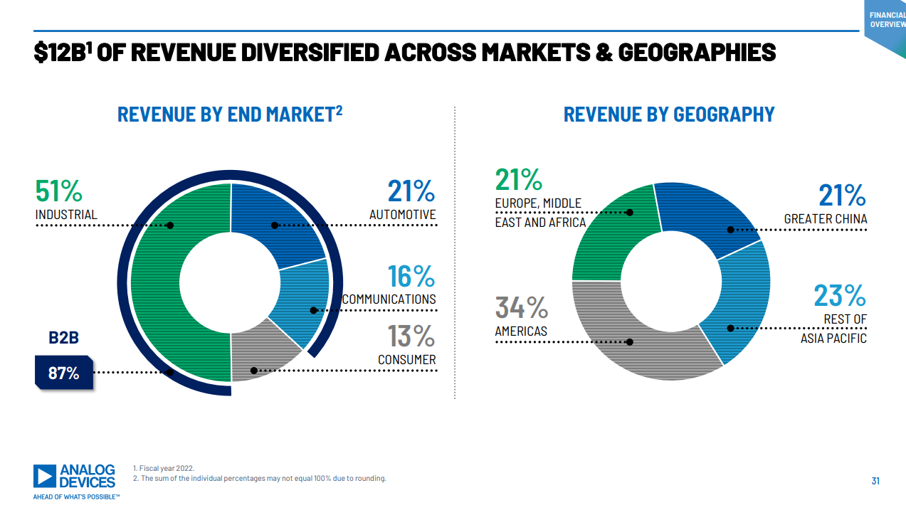
Analog Devices
Analog Devices Incorporated (ADI) is the second largest analog chip provider in the world.
ADI has focused on providing complete solutions to customers, providing both connected chips and services. This has enabled them to further entrench their moat and upsell customers. Historically, companies would buy components from a variety of suppliers and integrate those parts themselves.
In 2021, ADI acquired Maxim Integrated, another top 5 analog company in the world.
This slide from their investor’s report gives good insight into their business:
Conclusion
I’d like to end by providing some perspective on how the market values the industry.
From a market cap perspective, Nvidia dominates the market.
All of these companies are among the 200 largest companies in the world by market cap.
I find it fascinating how little we hear about these companies.
They are the foundation for every technological advancement we’ve seen over the last 50 years. They will continue to be the foundation of technology for years to come.









Great job Eric.
Its a complex industry but a very interesting one and also one of the most important industries, if not the most important industrie.
Asianometry and also Chipstockinvestor.com are good resources to understand the Semiconductor industry
I'm learning about the semiconductor Ecosystem for 2 years now, also invested.
An ETF like SMH can be a good idea to start.
Good overview, you made it less complicated 😉