
A Primer on EDA: Software for Semiconductors
The first in a several-part series on the history, technology, markets, and outlook for one of the most important software industries in the world.

Cadence and Synopsys have been two of the best-performing stocks in the world over the last decade. Cadence and Synopsys have compounded annually at ~33% and ~29%, respectively (excluding dividends).

They’ve become two of the most defensible software companies in the world in addition to being an important strategic asset for the US.
Today, their narrative is abundantly positive. Ten to 15 years ago? The path forward wasn’t so clear.
Especially for Cadence, who struggled with pricing and execution in the 2000s, they got to the point where they were exploring a private equity takeover by KKR. Lip-Bu Tan took over the business in 2009, and the stock’s been mostly a rocketship since.
In true expectations-investing-style, low expectations + great fundamental performance created this incredible situation for returns.
While the phrase “the most important company you’ve never heard of” has been overplayed, Synopsys and Cadence Design Systems are certainly in that conversation. These two companies (along with Siemens EDA) have an oligopoly on the electronic design automation (EDA) industry, the software used to design semiconductors.
Every major semiconductor company in the world uses this software. This means every major piece of technology we use relies on these companies.
This has led to Synopsys and Cadence (1) returning some of the strongest returns in the market over the last decade and (2) having some of the highest valuations in the market.
This will be the first in a several part series on the Electronic Design Automation (EDA) industry, its major players, and what its future may look like.
1. An Overview of EDA & Where it Fits in the Semiconductor Ecosystem
Electronic design automation (EDA) tools are the software used to design semiconductors. Semiconductor design firms like Nvidia will use these tools to design chips and simulate their performance before being fabbed by TSMC.
They also sell “building blocks” of semiconductor IP. When a firm is designing a chip, instead of redesigning Wi-Fi and USB interactions, they can buy the IP for that functionality and include it in their design. We can see where they fit into the ecosystem below:
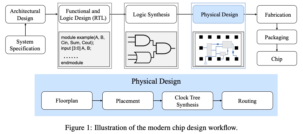
The process of designing a semiconductor is as follows:
1. Requirements Gathering & System Design
As with other physical products, the first step in designing chips is defining what they must accomplish. What will the chip do, how will it be used, and what performance metrics need to be met to achieve those goals? This is all driven by what customers are demanding and the use cases for the chip.
Companies will define specification sheets with all requirements before moving to design.
2. Logic Design & RTL (Register Transfer Level) Coding
Next, a team of designers will start the logic or circuit design. They will specify the high-level building blocks of the chip and define the logic of those building blocks using a coding language like Verilog.
These building blocks include blocks like logic circuits, memory circuits, and I/O interfaces that manage the flow of data in and out of the chip. The RTL design must define how data will flow through the chip; for example, a logic block will need data from different memory blocks, and these operations must be synchronized across the chip.
The end result is a “blueprint” of the logic and memory circuits wired together.
3. Logic Synthesis
Since chips are too complex to design every circuit by hand, designers use logic synthesis tools to turn that RTL code into a “netlist” of gates creating the logical representation of the chip. These gates create the pathways for the semiconductor to process information, consisting of logical functions like (AND, OR, NOR) and flip-flops (memory units either in a 1 or 0 state):
4. Physical Circuit Design
After logic design, the netlist goes to physical design which is made up of four primary steps: Floorplan, Placement, Clock Tree Synthesis, and Routing.
Floorplanning lays out the approximate position of large blocks (logic, memory) on the chip to minimize wire length, area, and power consumption. Placement determines the exact position of cells (logic gates and flip-flops) within the large blocks.
Clock Tree Synthesis creates a distribution network to optimize the circuit’s data flow for timing. For example, if a logic circuit needs data from several memory units, the data should arrive at the logic circuit at the same time. Data buffers or inverters are inserted to distribute clock signal across the chip. Finally, Routing lays out the wiring on the chip to minimize wire length, and minimize “crosstalk” and “parasitic” effects within the chip.
5. Simulation, Verification, and Validation
Once the chip has been designed, it will be simulated to ensure it meets performance requirements and doesn’t violate the design rules of fabs like TSMC.
The chip will undergo many verification steps, including design rule checking, layout validation, timing analysis, and foundry rule analysis. If any rules are violated, the design will be revised and re-verified.
The cost of design flaws will be in the tens of millions, and can climb into the hundreds of millions the longer the product is delayed.
Verification is one of the key bottlenecks in semiconductor design, and there are typically 1-2 verification engineers for every designer. Because of these high demands and rapid semiconductor product cycles, there’s a meaningful talent shortage for verification engineers.
6. *Bonus: PCB Design:
Printed Circuit Board (PCB) design is the process of designing how semiconductors will fit into a broader system. While chip design focuses on creating the semiconductor itself, PCB design deals with the circuit board of the entire system, connecting the chip to other components like memory/wifi/analog chips, LED lights, buttons, and sensors.
The process is similar to the chip design process but is simpler (still not easy) and uses a different toolset. The customer base is much different in this industry as well because many companies design electronics while relatively few design semiconductors.
2. A Brief History of EDA Software
Much of this section came from the following sources, all are worth checking out (Asianomtery, Early History of EDA, a Brief History of EDA).
The Early History of EDA
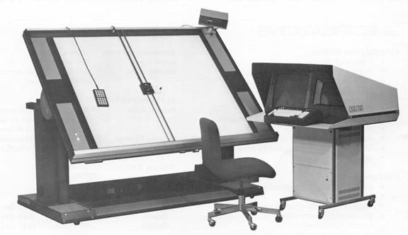
Prior to EDA software, semiconductors were designed by hand using drafting tools, rulers, and paper, which were then manually transferred onto photomasks (used in projecting the design onto semiconductors). The first versions of EDA software were developed internally at large tech companies like IBM and AT&T (much of modern technology can be traced back to the research labs of these two companies.)
The 1970s saw the emergence of the first generation of standalone EDA companies: Applicon, Calma, and Computer Vision. Calma, founded in 1965, created the Graphic Design System (GDS) series of tools for circuit design. These would become the industry standard for design in the 1970s. They allowed designers to digitize physical designs and view/edit them via the attached terminal.
Into the 1980s, semiconductors continued to increase in transistor density (via Moore’s Law). That first generation of companies struggled to adapt, so the next generation of companies rose with Mentor Graphics, Valid, and Daisy Systems.
In the 1980s, workstations and PCs rose in popularity transforming how users interacted with software. For the first time, companies could sell just software installed on workstations and PCs, instead of integrated hardware and software.
Enter the Fabless Business Model
At the same time, the semiconductor industry was restructured starting in the late 1980s. Before this, semiconductor firms were mostly vertically integrated, meaning they did their design and manufacturing in-house. Many used in-house design tools to design chips as well.
With the introduction of the fabless business model, this all changed. Companies could now outsource their manufacturing, SIGNIFICANTLY reducing the barrier to entry of designing a chip. At the same time, Synopsys (1986) and Cadence (1988) were founded, following the definition of a market-expanding technology. Companies could now design chips with cutting-edge software and outsource their manufacturing to TSMC (founded 1987).
Since then, the disruption that was the fabless model has only gotten stronger. TSMC did $70B in revenue last year, while Intel, the last major IDM in logic semiconductors, faces the most significant struggles in its history.
Industry Consolidation
Synopsys introduced the first commercially successful logic synthesis tool in 1986. This allowed engineers to focus on high-level design while letting the synthesis tool act as a compiler for those instructions. (Interestingly, we may be seeing something similar happen today with AI coding tools).
Cadence was founded in 1988 as a merger of SDA systems and ECAD, and would create a new generation of “place and route” software.
Over the next decade, Synopsys would gain momentum in the “front end” (synthesis) of semiconductor design while Cadence would own the “back end” of design (layout, verification).
From the 1990s today, we’ve seen the consolidation of the EDA industry onto Synopsys, Cadence, and Siemens EDA (Mentor Graphics):

This has happened, in large part, for three reasons:
1. The increasing complexity of semiconductors made it increasingly difficult to maintain technical advantage at the leading edge.
2. Synopsys and Cadence aggressively made acquisitions to consolidate their position (Cadence even tried to acquire Synopsys).
3. The competitive advantages of Synopsys and Cadence made it difficult for new entrants to enter the market. The technical complexity, switching costs, and GTM challenges prevented startups from challenging the incumbents.
These trends continue to today, providing the fundamental structure of this industry: a duopoly, with one player in third place, and no clear path to that changing.
3. An Overview of EDA Markets
The market is dominated by a few oligopolistic players, with some smaller niche providers, and some startups taking on the market.
The Oligopoly: Synopsys, Cadence, and Siemens EDA (formerly Mentor Graphics)
Synopsys is the largest company in this space, with revenue of $6.2B in the last 12 months. They’re about to get larger, acquiring the fourth largest player in EDA software, Ansys for $35B. Ansys had revenue of $2.5B over the last 12 months, although most of that came from simulation software; even their EDA segments are mostly chip simulation software. Approximately 70% of Synopsys’ revenue comes from EDA while ~30% comes from IP.
Cadence is the second largest player in the space, with $4.4B in revenue in the last 12 months. Approximately 90% of Cadence’s revenue comes from EDA tooling, while the last ~10% comes from IP.
Both Synopsys and Cadence offer a full platform for EDA software, meaning companies could design a chip entirely on their platforms. However, nearly every large semiconductor company uses both products for specific workflows. The next largest revenue item is IP, where they sell pre-designed blocks of semiconductors.
Siemens EDA is the third player in this space, through acquiring Mentor Graphics for $4.5B in 2016. Siemens often gets lost in this conversation, as EDA is a small piece of their revenue. They have an integrated systems approach offering software (EDA & CAD) and hardware (PLCs are a large segment for them - essentially computers for manufacturing lines). For context, Siemens does $80B+ in revenue and is valued at ~$164B as of December 12th, 2024.
Here’s an interesting graphic on these companies strengths in specific EDA verticals:

Fundamentals & Multiples
Two charts tell the story of the returns we’ve seen from Cadence & Synopsys. First, their revenue has grown nicely (but not incredibly) over the last decade (SNPS - 12% CAGR, CDNS - 10% CAGR):

Secondly, their multiples have grown almost incredibly well (SNPS - 16.2% CAGR, CDNS - 20.1% CAGR).

Over the last decade, these companies have become increasingly attractive businesses, transitioning from license-based pricing to subscription-based pricing. This, combined with consolidating market shares and semiconductor growth, led to the fairly incredible rise of their multiples in addition to their revenue.
Both companies have seen profit margins increase over the last decades, but Cadence has significantly expanded its gross margin. It paints the picture of their metrics today: Cadence is a slightly more efficient business on a slightly smaller scale.

Startup Ecosystem
Finally, several startups are taking on the market, with most focusing on PCB design.
Candidly, this has been a tough space for startups. As I described in my last piece on physical design software, we have three really entrenched moats in physical design software, including EDA software:
Technical complexity: This is some of the most complex software in the world. EDA software, for example, has millions of lines of code for each tool. Startups can spend 5+ years just hitting feature parity for CAD platforms. So, while it’s hard to build these tools that are just as good, it’s even harder to build tools that are better.
Switching costs and risks: Do companies want to risk moving their decades of IP and retraining employees? The complexity of the software means moving tools requires significant retraining time, meaning less productivity time and potential downtime. Plus, if design flaws result from switching software, the costs are much higher than software defects.
The GTM problem: Most Fortune 100 hardware and adjacent companies use these tools and have little reason to move. Mid-market and SMBs have Autodesk as a standard, which is taught in schools, and engineers spend years getting certified in it. These are industry defaults. There aren’t many scaled consumer use cases, so the bottom of the market doesn’t provide much value. This means there’s no good place for a company to start selling.
We’re seeing a few approaches taking on this market, most of them are taking on the PCB market, not the EDA market. This is because many smaller customers use PCB design software, and any company designing electronics will need this software.
With that being said, there’s an excitement around AI & Chip Design that will open the door for any startup that can provide real technical outperformance to the market. They’ll be able to collect funding, hopefully form partnerships for data access, and will have the opportunity to build a large business.
4. Some Thoughts on This Space:
1. A quick note on investment prospects:
At these valuations, it’s hard to see a strong risk reward from Synopsys or Cadence. Both are historically great software businesses: strong moats, strong margins, and strong growth. However, if we view multiples as a probabilistic distribution, the probabilities of lower multiples moving forward are high. If prices get more favorable moving forward, they become more attractive investment opportunities.
2. Competition is ~very~ important in this field.
The moats of Synopsys and Cadence are probably the strongest in software, but startup success is important to the field of AI as a whole. For one, the space is very strategic to the US’ semiconductor advantages. More competition, more innovation, more opportunity for really smart people to be successful is better for everyone. Startups help drive that competition and innovation forward.
3. Does generative AI for design provide the next level of abstraction?

I think this may be the most interesting question in the space. We’ve started to see this with AI coding, with developers coding in natural language now. The programming language gets abstracted away as developers focus on the logic and architectures that deliver performance improvements.
So, AI won’t blindly solve our problems, but we do continue to see progress with AI in EDA from Synopsys, Cadence, Google, Nvidia, and a host of startups innovating here. I think the excitement around AI, the willingness to adopt new solutions, and the increased funding available for startups is accelerating this innovation.
AI in this field is one of the most challenging and interesting applications of AI. Better AI EDA software = better AI hardware = better AI EDA software. All roads lead through EDA software!
Because I think it’s such an important problem, my next EDA article will feature a deep dive on AI/LLMs for chip design.
As always, thanks for reading!
Disclaimer: The information contained in this article is not investment advice and should not be used as such. Investors should do their own due diligence before investing in any securities discussed in this article. While I strive for accuracy, I can’t guarantee the accuracy or reliability of this information. This article is based on my opinions and should be considered as such, not a point of fact. Views expressed in posts and other content linked on this website or posted to social media and other platforms are my own and are not the views of Felicis Ventures Management Company, LLC.
Great article. Has some background but this was well worth the read. I wonder about potential innovation as well in leveraging AI for better EFA software.
this is awesome!